Category: Science & Technology | Economy Relevance: GS Paper III — Indigenization of Technology, Industrial Policy, Infrastructure, Employment Source Desk: Current Affairs Desk, Vivechna IAS & Judiciary Academy
Context
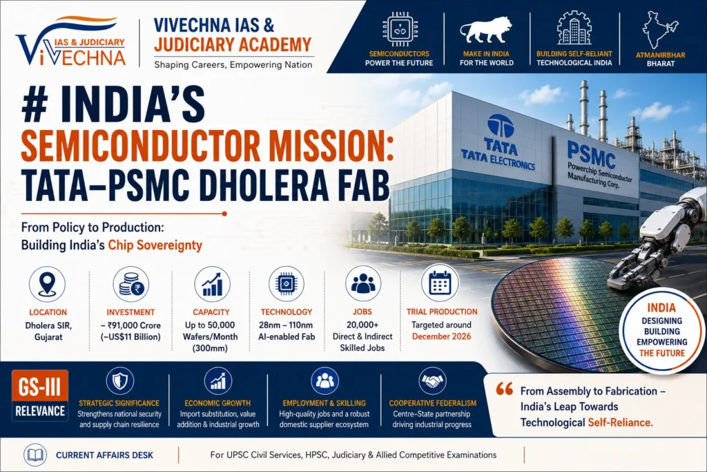
India’s chip-manufacturing push has moved decisively from policy announcement to physical construction. At Dholera in Gujarat, the Tata Electronics–PSMC semiconductor fabrication plant — the country’s first full-scale chip fab — has crossed the halfway mark in construction, with trial production targeted around December 2026. Union Electronics Minister Ashwini Vaishnaw has indicated that four semiconductor plants will be operational by the end of 2026, two more in 2027, and India’s first complete fabrication unit will be ready at Dholera by 2028. For UPSC aspirants, this is a live, evolving story that touches Polity (Centre-State cooperation, SEZ notifications), Economy (import substitution, capex subsidies), and S&T (strategic technology self-reliance).
What is the India Semiconductor Mission (ISM)?
- Established in December 2021 under a ₹76,000 crore incentive framework.
- Administered by the Ministry of Electronics and Information Technology (MeitY).
- Offers fiscal support of up to 50% of project cost as capital subsidy for approved silicon fabs, compound semiconductor units, OSAT/ATMP (assembly, testing, marking, packaging) facilities, and chip design projects.
- As of mid-2026, the Centre has approved 13 semiconductor projects across seven states, with cumulative investment commitments running into lakhs of crores of rupees.
The Tata–PSMC Dholera Fab: Key Facts
| Parameter | Detail |
|---|---|
| Location | Dholera Special Investment Region (SIR), Gujarat |
| Partners | Tata Electronics (Tata Sons subsidiary) + Powerchip Semiconductor Manufacturing Corporation (PSMC), Taiwan |
| Total Investment | Approx. ₹91,000 crore (~US$11 billion) |
| Capacity | Up to 50,000 wafer starts per month (WSPM) |
| Wafer Size | 300mm (12-inch), AI-enabled fab with factory automation |
| Process Nodes | Starting at 28nm, with roadmap covering 28nm–110nm (mature-to-advanced range) |
| Products | Power management ICs, display drivers, microcontrollers (MCUs), high-performance computing chips for AI and automotive electronics |
| Jobs | Over 20,000 direct and indirect skilled jobs |
| Government Support | 50% fiscal support (pari-passu) under ISM; additional state-level capital subsidy from Gujarat |
| Technology Partner (lithography) | Netherlands-based ASML, for advanced lithography systems |
| Trial Production | Targeted around December 2026 |
| Full Commercial Scale-up | Projected through 2027–2028 |
Note: PSMC is not the same as TSMC. It is a Taiwanese foundry specialising in mature-to-advanced nodes (28nm–90nm range) and specialty DRAM/power-management chips — not leading-edge 2nm logic. This node range, however, covers the majority of chips India currently imports for automotive, industrial, and consumer electronics use.
Wider Semiconductor Ecosystem Building Up Around It
- Micron Technology’s ATMP facility, Sanand (Gujarat): Inaugurated by the Prime Minister in February 2026 — the first operational facility of the current mission cycle, focused on packaging DRAM and NAND flash memory chips.
- Kaynes Semicon OSAT, Sanand: Reached commercial production in March 2026, focused on chip testing and packaging.
- CG Power OSAT unit, Sanand: Scaling high-volume assembly and testing.
- Tata Semiconductor Assembly and Test (TSAT), Jagiroad, Assam: India’s northeastern semiconductor packaging hub.
- SiCSem’s Silicon Carbide fab, Bhubaneswar (Odisha): India’s first commercial SiC compound semiconductor facility.
- Supporting ecosystem: INOX Air Products is setting up a specialty ultra-high-purity gas facility in Dholera, and Dholera has been granted SEZ status, reflecting the maturing industrial cluster around the fab.
Why This Matters for GS-III (Mains Relevance)
1. Strategic and National Security Angle Semiconductors are foundational to defence systems, telecom networks, satellites, and critical infrastructure. Domestic fabrication reduces India’s dependence on a handful of overseas suppliers concentrated in Taiwan, South Korea, and China — a vulnerability starkly exposed during the 2021 global chip shortage.
2. Import Substitution and Economic Value Addition India currently imports the vast majority of its semiconductor requirements. A domestic fab targeting the 28nm–110nm range directly addresses chips used in automobiles, consumer electronics, and industrial systems — segments with high import volumes.
3. Employment and Skilling Beyond the 20,000+ direct and indirect jobs at Dholera, the mission is building a skilled technician base and a domestic supplier ecosystem (gases, chemicals, precision engineering) — relevant to the “demographic dividend” debate in current affairs.
4. Centre-State Cooperative Federalism The Fiscal Support Agreement model (Centre + Gujarat government layering subsidies) is a useful example for questions on cooperative federalism in industrial policy.
5. Make in India, For the World The mission reflects India’s shift from an assembly/packaging-only role (OSAT) to attempting front-end fabrication — a more complex and higher-value stage of the semiconductor supply chain.
Possible Prelims Pointers
- India Semiconductor Mission was launched in 2021 with a ₹76,000 crore outlay, administered by MeitY.
- The Tata–PSMC Dholera fab is being built as a 300mm, AI-enabled facility.
- PSMC stands for Powerchip Semiconductor Manufacturing Corporation, a Taiwanese foundry.
- OSAT = Outsourced Semiconductor Assembly and Test; ATMP = Assembly, Testing, Marking, and Packaging.
- Micron’s Sanand facility was inaugurated in February 2026.
Possible Mains Question
“India’s semiconductor mission marks a shift from policy intent to industrial execution. Critically examine the strategic significance of domestic chip fabrication for India’s technological self-reliance and economic security.” (GS-III, 15 marks)
Structuring tip: Introduction (context of Dholera fab) → Strategic significance (defence, supply chain resilience) → Economic significance (import substitution, jobs, value addition) → Challenges (capital intensity, talent gap, dependence on foreign lithography/technology transfer, execution risk) → Way forward (design ecosystem, R&D investment, skilling) → Conclusion.
Prepared by the Current Affairs Desk, Vivechna IAS & Judiciary Academy, for UPSC Civil Services, HPSC, and allied competitive examinations.